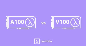

Lambda customers are starting to ask about the new NVIDIA A100 GPU and our Hyperplane A100 server. The A100 will likely see the large gains on models like GPT-2, GPT-3, and BERT using FP16 Tensor Cores.
For language model training, we expect the A100 to be approximately 1.95x to 2.5x faster than the V100 when using FP16 Tensor Cores.⁴
You should expect to see a wide range of performance speedups based on the model that you're training, the floating point representation you use, the theoretical peak attainment of the Tensor Cores, and the ability to leverage the new sparsity feature. The speedup over the V100 could be anywhere from 1.25x to 6x according to published numbers from NVIDIA.
NVIDIA A100 GPU vs NVIDIA V100 GPU
| A100 | V100 | |
|---|---|---|
| Language Model Training Speedup over V100 using FP16 TC | Up to 2.5x⁴ | 1x |
| TF32 Tensor Core Peak Theoretical Performance | 156 TFLOPS | N/A |
| FP16 Tensor Core Peak Theoretical Performance | 312 TFLOPS | 125 TFLOPS |
| FP32 Peak Theoretical Performance | 19.5 TFLOPS | 15.7 TFLOPS |
| Die Size (mm²) | 826 sq. mm | 815 sq. mm |
| Process Node | TSMC 7nm | TSMC 12nm FFN |
| TDP | 400 W | 300 W |
| TF32 GFLOPS / watt | 390 GFLOPS / watt | N/A |
TensorFloat-"32" - a 19-bit representation
TensorFloat-32 (TF32) is a 19-bit floating point representation that's natively supported by the A100's tensor core elements. A TF32 representation looks like this:
- 8-bit exponent (similar to standard FP32 and bfloat16)
- 10-bit mantissa (similar to standard FP16)
- 1-bit sign
No code changes required
Your TensorFlow/PyTorch code will still use FP32. However, within the tensor cores, these numbers are converted to TF32. Here's how it works:
- The tensor cores will receive IEEE 754 FP32 numbers.
- The tensor cores will convert the FP32 numbers into TF32 by reducing the mantissa to 10-bits.
- The multiply step will be performed in TF32.
- The accumulate step will be performed in standard FP32, resulting in an IEEE 754 FP32 tensor output.
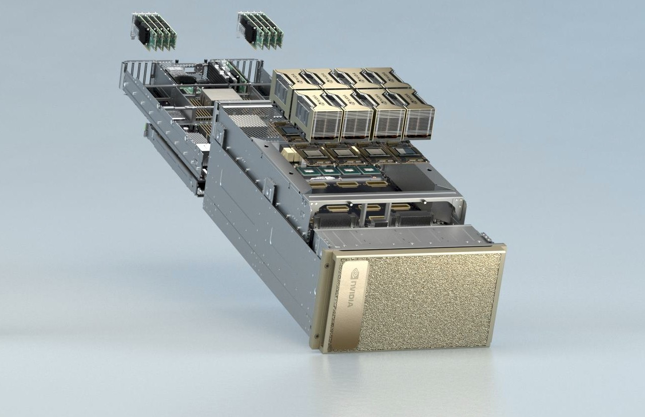
The DGX A100 Server: 8x A100s, 2x AMD EPYC CPUs, and PCIe Gen 4
In addition to the NVIDIA Ampere architecture and A100 GPU that was announced, NVIDIA also announced the new DGX A100 server. The server is the first generation of the DGX series to use AMD CPUs. One of the most important changes comes in the form of PCIe Gen 4 support provided by the AMD EPYC CPUs. This allows for the use of Mellanox 200 Gbps HDR InfiniBand interconnects. 16 lanes of PCIe Gen 3 has a peak bandwidth of 16 GB/s while 16 lanes of PCIe Gen 4 offers twice the bandwidth, 32 GB/s.
This is important for three reasons:
- CPU to GPU communication will be twice as fast when compared with previous generations of servers.
- PCIe Gen 4 enables the use of the new Mellanox 200 Gbps HDR InfiniBand interconnects. HDR Infiniband (200 Gbps) provides a peak bandwidth of 25 GB/s. As you can see: 32 GB/s provided by PCIe Gen 4 > 25 GB/s required by Mellanox HDR Infiniband > 16 GB/s provided PCIe Gen 3.
- The new GPUDirect Storage feature, which allows GPUs to read directly from NVMe drives, will be able to support twice as many NVMe drives using PCIe Gen 4 when compared with PCIe Gen 3. For more info on GPUDirect Storage, see NVIDIA's post here: https://devblogs.nvidia.com/gpudirect-storage/.
Let's take a look at the DGX A100 server side by side with the DGX-1 and Lambda Hyperplane-8 V100.
| DGX A100 | DGX-1 | Lambda Hyperplane-8 V100 | |
|---|---|---|---|
| Theoretical TF32 Tensor Core TFLOPS | 156 TFLOPS | N/A | N/A |
| Theoretical FP32 TFLOPS | 19.5 TFLOPS | 15.7 TFLOPS | 15.7 TFLOPS |
| Theoretical FP16 Tensor Core TFLOPS | 312 TFLOPS | 125.6 TFLOPS | 125.6 TFLOPS |
| FP16 TC Megatron-BERT Training Performance | 1.95x | 1x | 1x |
| PCIe Generation | 4 | 3 | 3 |
| Interconnect Max Speed | 200 Gbps InfiniBand HDR | 100 Gbps InfiniBand EDR | 100 Gbps InfiniBand EDR |
| Interconnect Count | 9 | 4 | 4 |
| Total Interconnect Theoretical Throughput (Gbps) | 1800 Gbps | 400 Gbps | 400 Gbps |
| TDP (W) | 6500 W | 3500 W | 3500 W |
| Rack Units | 6 U | 4 U | 4 U |
| MSRP Price | $199,000 | $119,000 | $95,000 |
The DGX A100 offers far superior node-to-node communication bandwidth when compared with the DGX-1 or the Lambda Hyperplane-8 V100. We'll follow up in the future with an in depth benchmarking blog post comparing measured results of these systems. In addition, you might see the DGX A100 server provide better cluster scaling performance due to its massive increase in node-to-node communication bandwidth.
Deep Learning Focused Design Decisions
The A100 represents a jump from the TSMC 12nm process node down to the TSMC 7nm process node. Note the near doubling of the FP16 efficiency. This design trade-off maximizes overall Deep Learning performance of the GPU by focusing more of the power budget on FP16, Tensor Cores, and other Deep Learning-specific features like sparsity and TF32.
Conclusion
Like everybody else, we're excited about the new architecture, and can't wait to put the new A100 GPUs through their paces. We'll wait until we can perform independent benchmarks to make a conclusive statement on the overall performance. But, as we've seen from NVIDIA's language model training post, you can expect to see between 2~2.5x increase in performance when training language models with FP16 Tensor Cores.
Sources
- 18.1 TFLOPs is derived as follows: The V100's actual performance is ~93% of its peak theoretical performance (14.6 TFLOPS / 15.7 TFLOPS). If the A100 follows this pattern, its actual performance will be 18.1 TFLOPS (93% of 19.5 TFLOPS).
- 1.24x = 18.1 TFLOPS (est. of the A100's actual perf.) / 14.6 TFLOPS (the V100s measured perf.)
- "NVIDIA Ampere Architecture In-Depth."
- Language model training performance is based on benchmarks performed by NVIDIA. See: "State-of-the-Art Language Modeling Using Megatron on the NVIDIA A100 GPU."
Appendix
Die Size Analysis & Silicon Economics

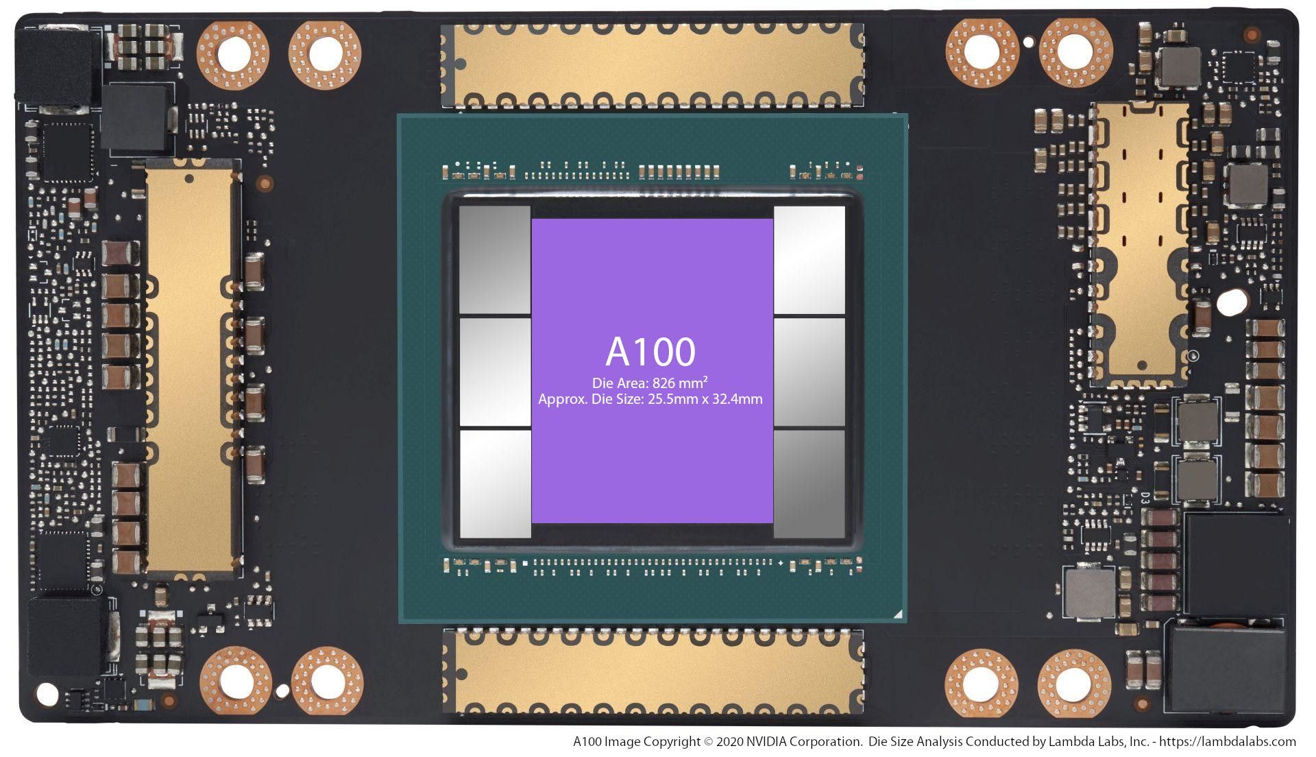
Using public images and specifications from NVIDIA's A100 GPU announcement and a knowledge of optimal silicon die layout, we were able to calculate the approximate die dimensions of the new A100 chip:
Known Die Area: 826 mm²
Die Size in Pixels: 354 px * 446 px
Die Aspect Ratio: ~0.793721973
dar = a / b
a * b = 826
a = 826 / b
dar = 826 / b^2
b^2 = 826 / dar
b = sqrt(826 / dar)
a = 826 / sqrt(826 / dar)

a = 826/sqrt(826/0.792792793) = 25.5899755
b = sqrt(826/0.792792793) = 32.2593656
We then lay a prototype die of (25.589 mm x 32.259 mm) across the known usable area of a 300mm silicon wafer. It's clear that there are four dies, (two on each side) that won't fit unless we shrink the width down to 25.5 mm. This then gives us a rough estimate of a potential die size of 25.5 mm x 32.4 mm. This gives a total area of 826.2 mm² and 64 dies per wafer.
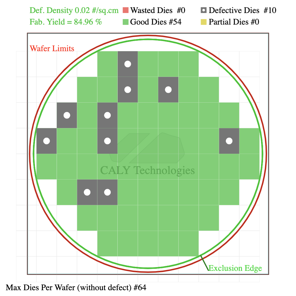
We conclude that the size of the A100 is approximately 25.5 mm x 32.4 mm and that they can fit 64 dies on a single wafer.
Lambda Hyperplane A100 Server
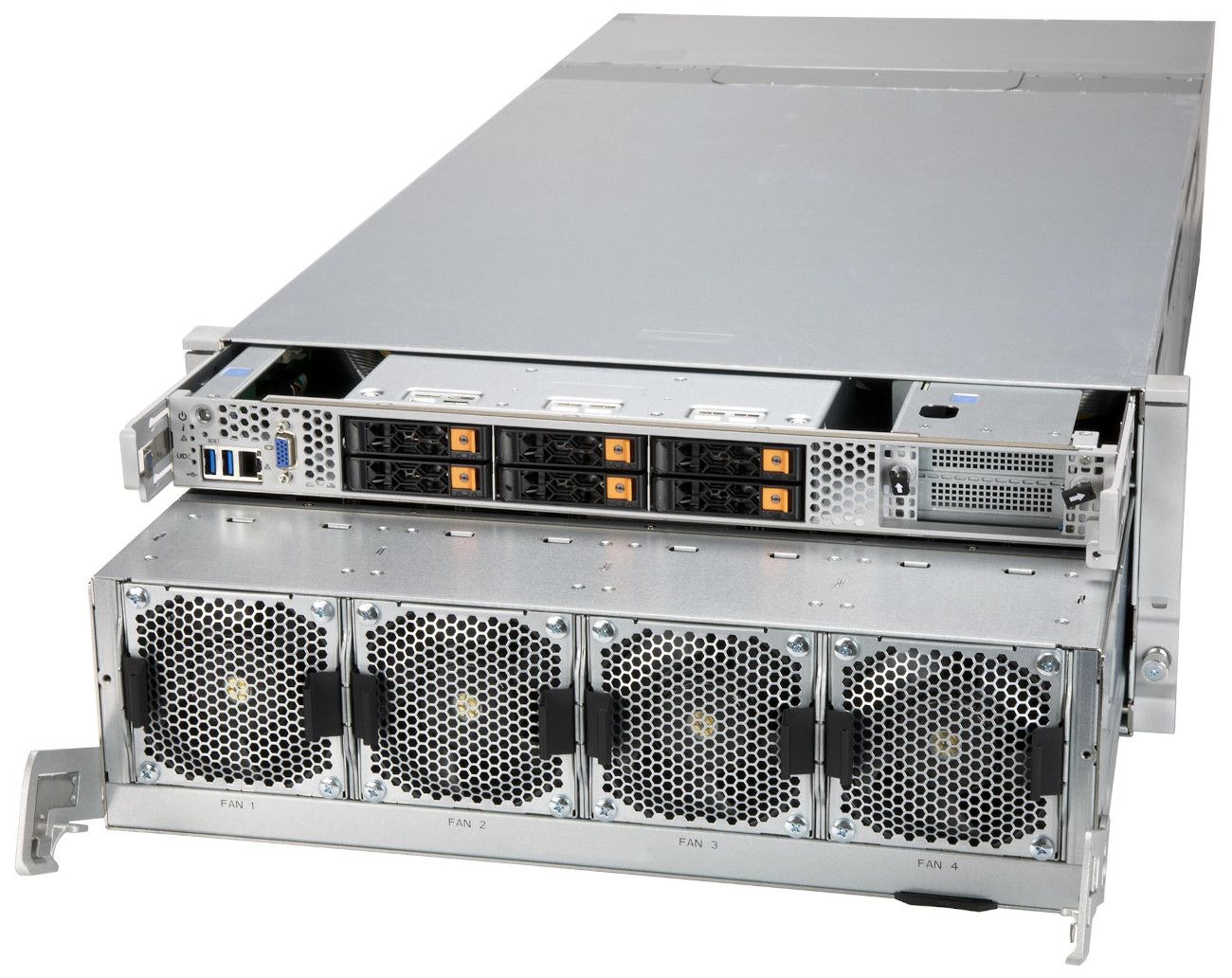
We're now accepting pre-orders for our Hyperplane A100 GPU server. Available in both 8x and 4x GPU configurations.